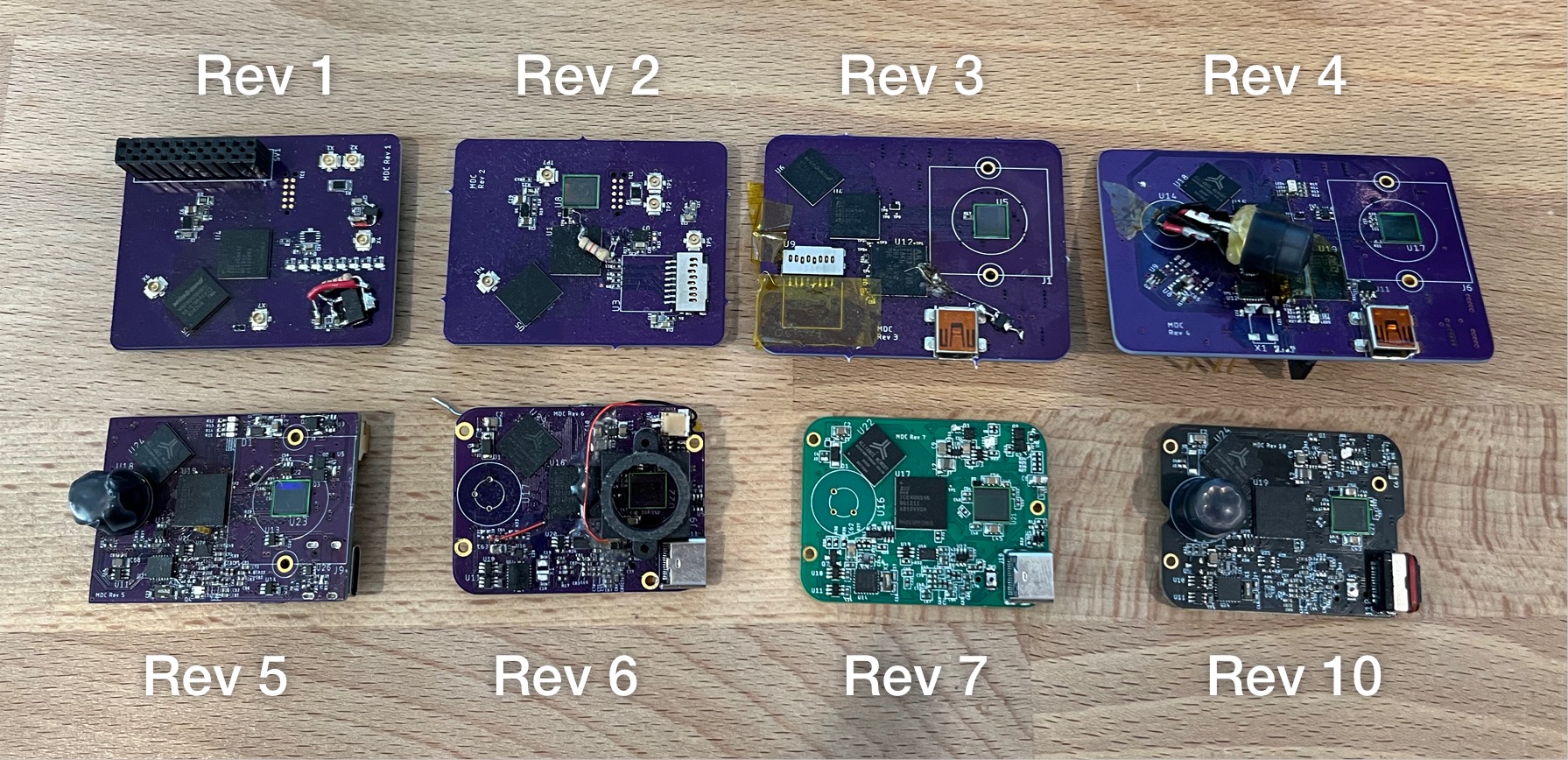
Revision 1
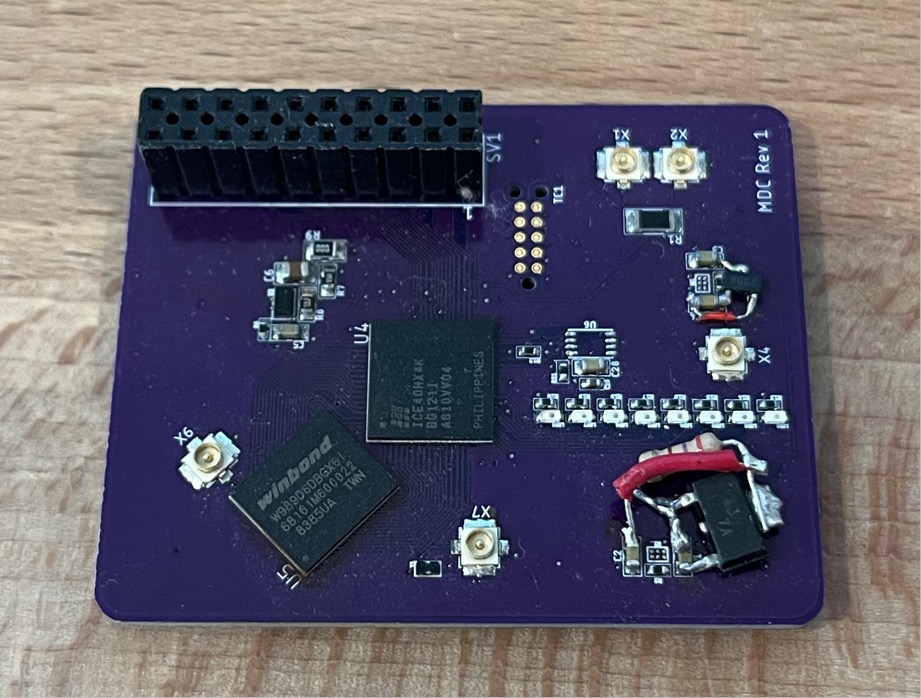
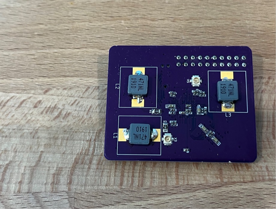
- get power supplies working
- get RAMController.v working with the SDRAM chip
- test different inductor sizes for power efficiency (larger inductors are more efficient with switching regulators, but take up more space)
This first revision didn't have an image sensor yet, so functionality was limited to reading/writing data to the SDRAM with the ICE40.
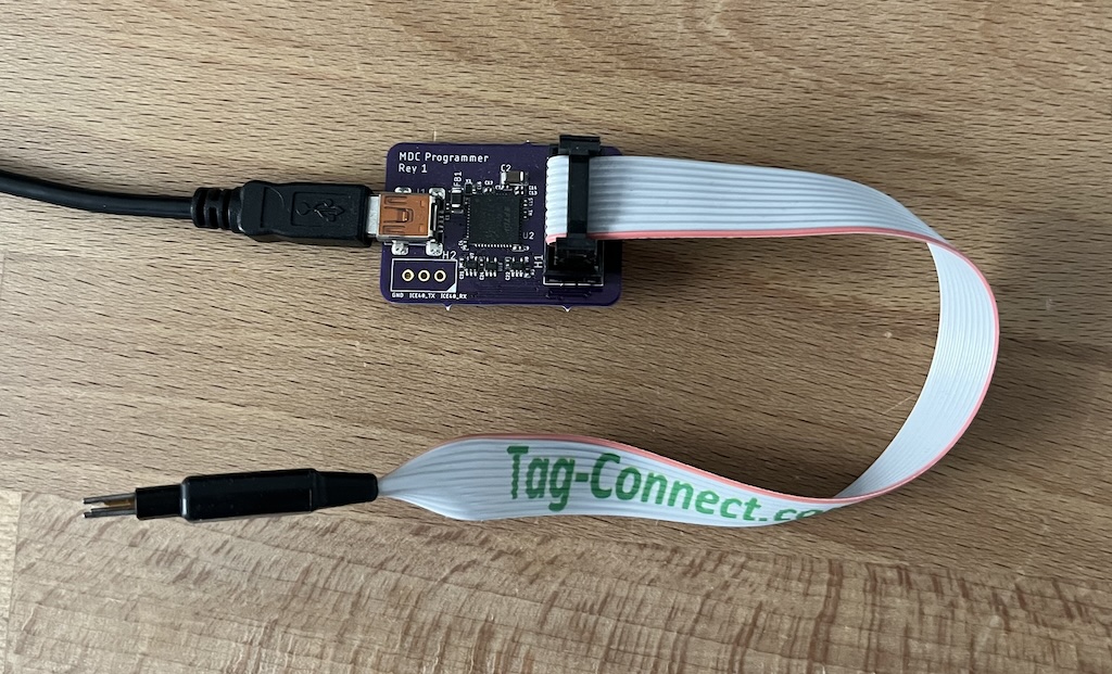
There was no USB connection on the first two revisions, so programming the ICE40 was done through a custom FTDI-based programmer, with a Tag-Connect connector:
Revision 2
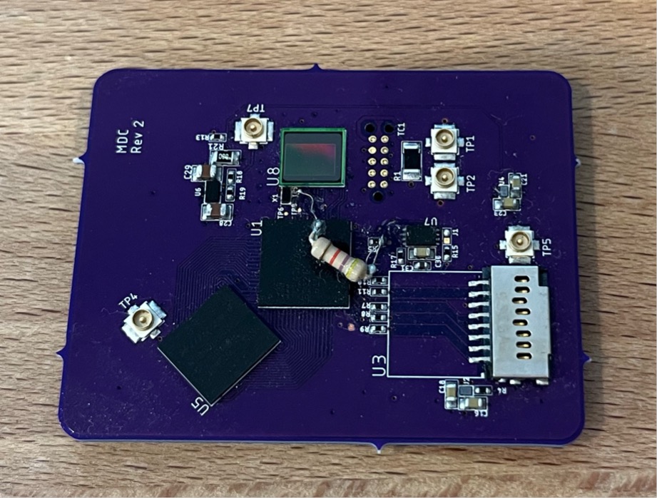
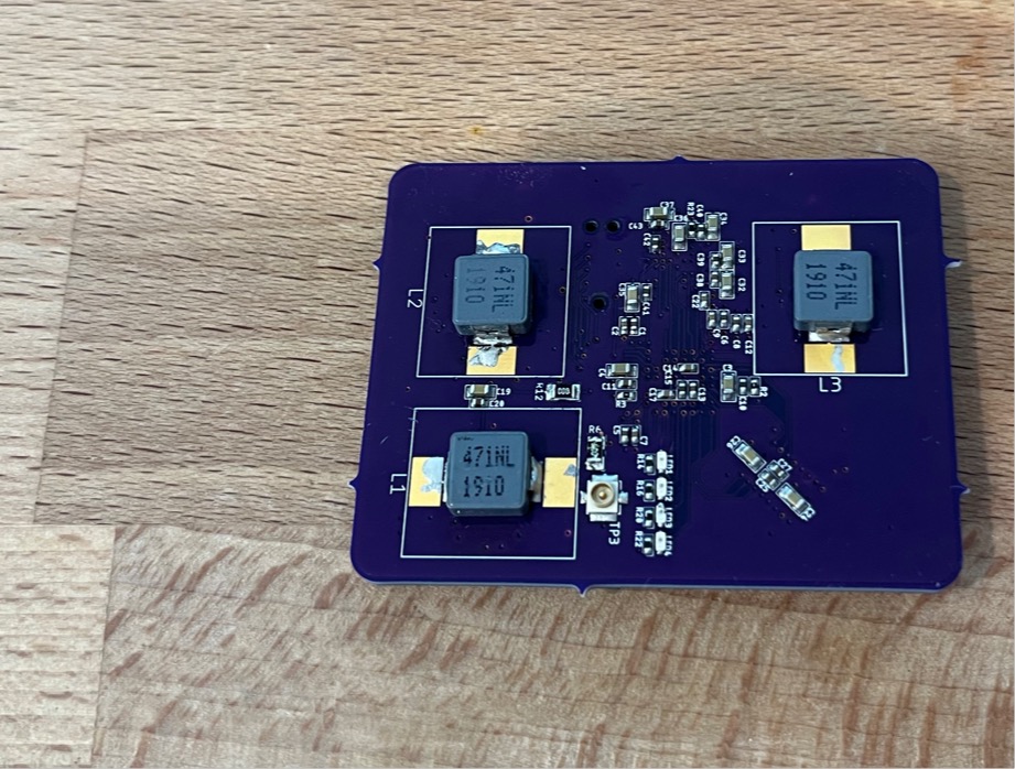
The second revision also added the flash chip for the ICE40 to maintain its programming across power cycles.
Revision 3
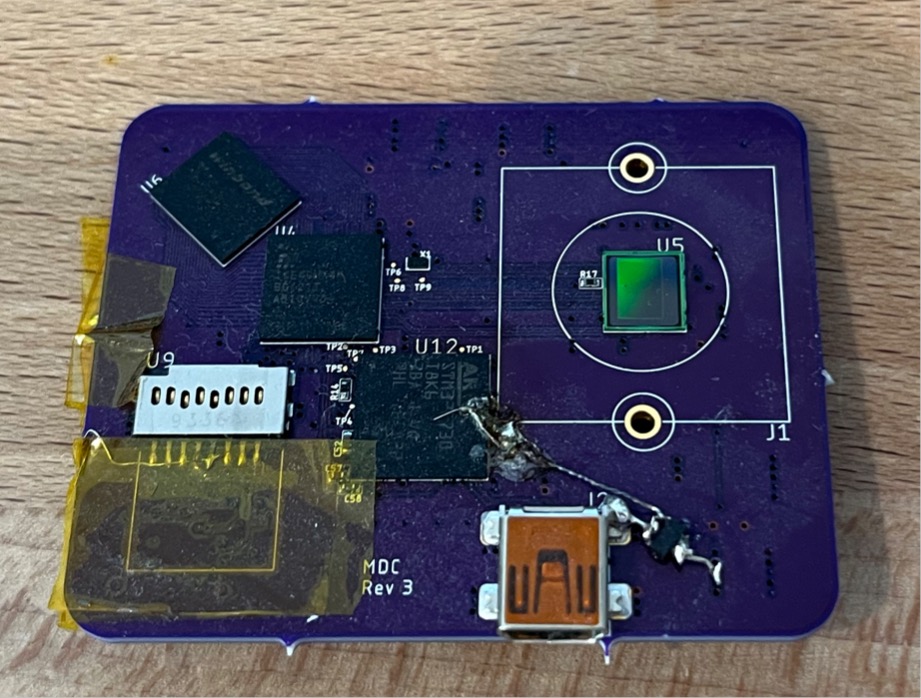
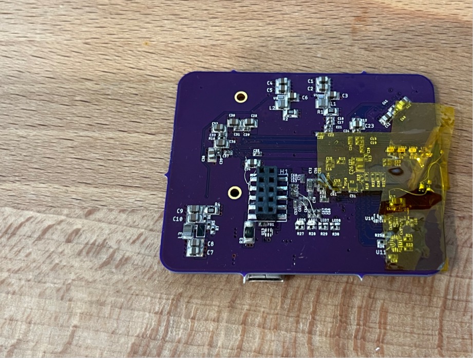
This revision also added mount points for a plastic lens socket that a standard M12 lens could screw into, so this board was the first revision that could capture clear imagery.
I made a mistake on one of the STM32's USB PHY pads, so to get USB working I had to route a bodge wire beneath the BGA STM32:
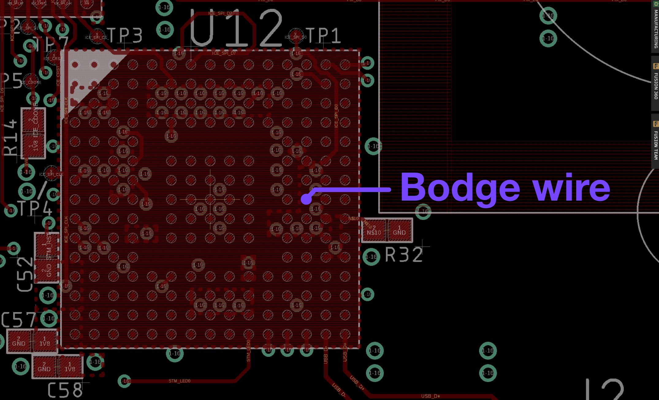
I had a hell of a time soldering that wire beneath the chip, which involved cutting a small "canal" into the PCB that the wire could rest in, and then soldering the BGA on top. Eventually I got it connected and added gobs of superglue to keep the delicate wire in place.
I also made some mistakes in the SD card wiring so I added bodge wires there too, hence all the Kapton tape.
Revision 4
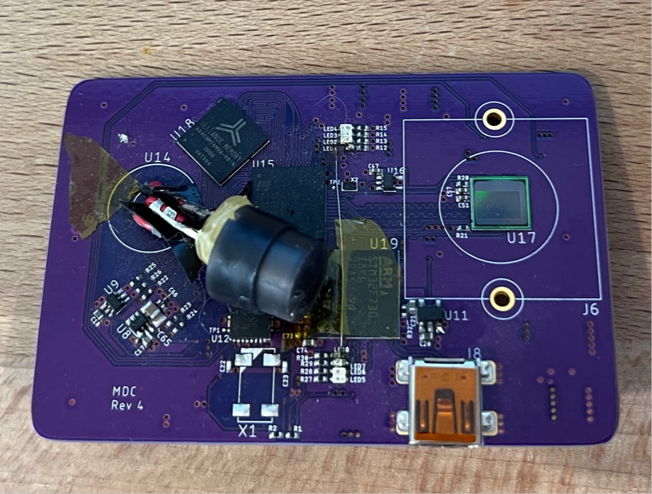
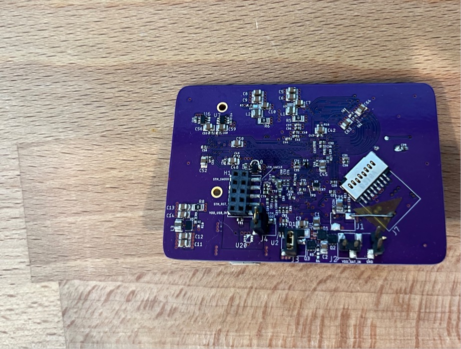
I messed up the footprint for the motion sensor (swapped VDD and GND, d'oh!) hence the motion sensor lying off to the side with bodge wires.
I also determined I needed an additional signal between the ICE40 and STM32 to facilitate high-speed data transfers, so I sacrificed a couple of debug LEDs to make that happen. (See the long bodge wire in the center of the board.)
Revision 5
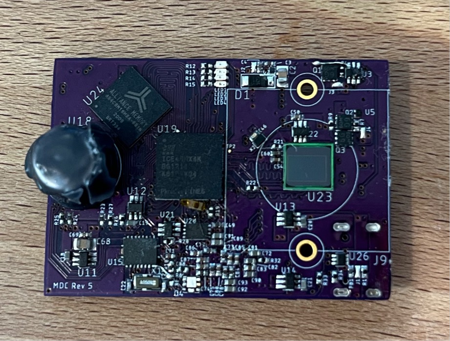
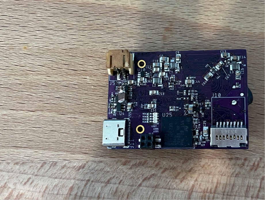
- shrink the PCB as much as possible (so the final device could be as small as possible)
- add support for being powered by a battery
- switch from USB-mini to USB-C
To support a battery I added the TPS2116 power multiplexer, to handle switching between USB power and battery power. To charge the battery while connected to USB, I added the MCP73831T lithium charge controller.
Revision 6
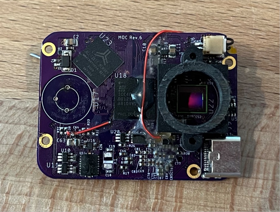
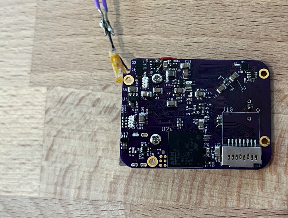
- shrunk the board further (from 46.5 to 44 mm wide)
- moved the USB-C receptacle from the back to the front of the board, to make more room for the battery
- replaced the battery connector with a smaller version to save space
- rounded the board corners to fit within the enclosure
- replaced the debug header with a Tag-Connect footprint
- added mount points to secure the PCB to the enclosure
Revision 7
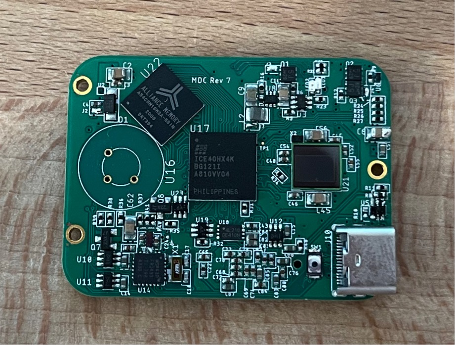
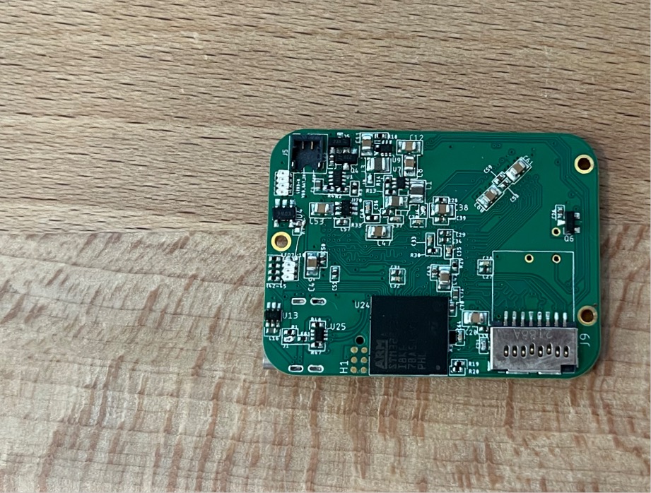
- added a tactile switch (pressed by the button that's mounted to the enclosure)
- added LEDs (red and green) to emit light through the enclosure lightpipe
- switched from MSP430FR2422 to MSP430FR2433 to go from 8 KB to 16 KB of FRAM (because the codespace was exhausted)
- removed the plastic lens housing to shrink the board further (the lens screws into the enclosure instead)
- reduced the number of PCB mount points from 4 to 3, to save space
- replaced the battery connector (again) to the low-profile Molex Pico-EZmate
Revision 8 & 9
These two revisions had some mistakes (eg a misplaced mount point relative to the enclosures that were already ordered) so I didn't end up assembling them.Revision 10
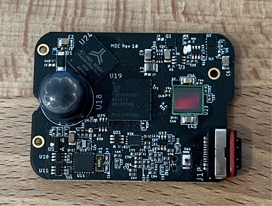
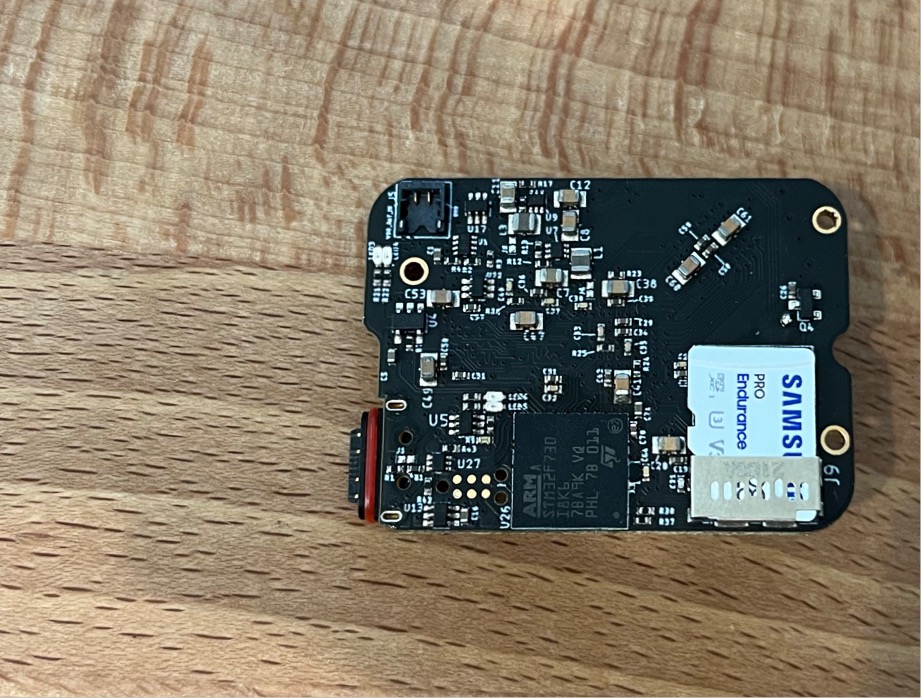
This final revision:
- replaced the USB-C receptacle with one featuring a waterproofing gasket
- moved the right mount point slightly
- rotated the Tag-Connect footprint to make it accessible while the PCB is mounted in the enclosure, so the STM32 can be programmed without removing the PCB
- switched the soldermask color to a swanky matte black
A Nasty Bug in the Production Hardware
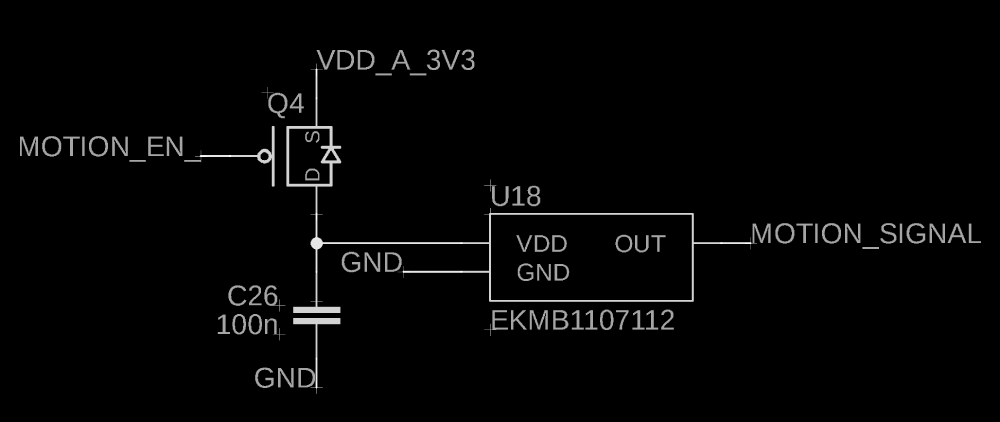
This final board had one nasty bug involving the motion sensor, which I only discovered after ordering 120 assembled boards. (I didn't discover it on revision 7 because I didn't bother to fit the motion sensor, because I didn't want to consume one — they cost $20 — and because the support circuitry is simple enough that I foolishly assumed there wouldn't be any issues.) The issue was that when the MSP430 enables power to the motion sensor using its MOTION_EN_ signal, it triggers an inrush current into the motion sensor and its bypass capacitor. This inrush current causes the VDD_A_3V3 rail to momentarily droop to 2.2V, which causes the MSP430 to brownout and reset:
A Firmware Hack to Fix it
This issue looked severe enough that it was going to require a hardware bodge to fix, but after spending a few days experimenting with firmware solutions I accidentally stumbled on one: For a little while (ie 100ms) before powering the motion sensor via MOTION_EN_, the MSP430 can enable a pullup resistor on the motion sensor's output signal MOTION_SIGNAL. This has the effect of slowly charging the motion sensor's internal nets to 3.3 V, so that the inrush current / voltage droop is prevented when MOTION_EN_ is enabled, and the MSP430 therefore doesn't brownout. No hardware modifications needed!
You can see this hack in action in the MSP430's source (search for "hack").
Lessons Learned
I learned a few lessons in designing Photon's PCB:- Be ambitious with prototype boards
My strategy with revisions 1-4 was to gradually add chips/subsystems to each revision until I had everything implemented. In hindsight this lead to a lot of unneeded board-assembly overhead without much gain. If I were to do this again, I'd add all the chips that I thought I needed to the first board that I assemble (so I'd effectively start with revision 4.)
- Don't be overly concerned about making mistakes on prototype PCBs
Just about every mistake I made on a PCB revision, I could correct with some clever bodging. Double-checking every single detail is too time-consuming and soul-sucking to be worth it.
- Add debug LEDs to microprocessors / FPGAs
When debugging microprocessors / FPGAs, it's invaluable to have a few LEDs to act as a single-bit
printf.These LEDs can also be sacrificed to get an extra GPIO that can be routed elsewhere with a bodge wire. (This approach saved the day in revision 4, where I needed to connect an extra GPIO between the ICE40 and STM32. Since both chips are BGAs, it would have been a pain to access an additional pad if not for a sacrificial debug LED.)
- Don't mass-produce a board until you've tested it
This is painfully obvious, but it bit me with the motion sensor issue in revision 10. If I had tested the motion sensor in the final revisions (the bug was introduced in revision 7, but I had only tested the motion sensor up to revision 5), I would've discovered that issue before ordering the final boards.
- Better tools are needed to ensure part footprints are correct
This isn't something that I can do differently, but it's certainly something on my wish-list. After encountering an error in a footprint for a part on GitHub, I started making my own footprints, but I inevitably make my own errors when doing it myself.
Error-free part footprints should be a solved problem.