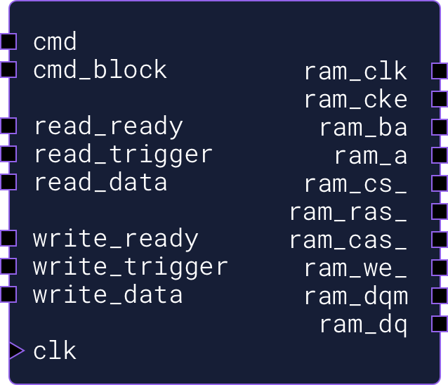
When synthesized for ICE40, RAMController.v's maximum clock frequency is ~130 MHz allowing for a maximum throughput of ~248 MB/sec. (These numbers are from Photon's top-level Verilog synthesized with the Yosys/icestorm toolchain.)
RAMController.v should work with any FPGA, but it's been specifically tested and used with the ICE40 and the Yosys/icestorm toolchain.
RAMController.v Overview
RAMController.v is a Verilog module that provides a simple interface for reading from / writing to single-port SDRAM chips.RAMController.v abstracts away the inconvenient details of managing an SDRAM, such as:
- initializing the SDRAM after power on
- issuing refresh commands at regular intervals (which might occur during a read/write)
- waiting the proper delays before/after reading/writing data
- activating the appropriate bank before reading/writing data, and precharging it after
- handling DQM masking on the appropriate clock cycle
RAMController.v breaks the SDRAM into a configurable number of "blocks". For example, Photon's SDRAM is large enough to hold two images, so it's broken into two blocks.
RAMController.v Interface
RAMController.v groups its IO signals into three ports, described below.Command Port
Reads and writes are initiated using the Command port:input wire[1:0] cmd, input wire[N:0] cmd_block,
- input cmd: the operation to perform
Valid values:
None,Read,Write,Stop - input cmd_block: the applicable block
Only applies for
cmd=Read/Write
Read Port
The Read port is used after aRead command is issued on the Command port. output wire read_ready, input wire read_trigger, output wire[N:0] read_data,
- output read_ready: signals whether
read_dataholds a valid word - input read_trigger: signals whether reading should advance to the next word on the next cycle
- output read_data: provides the word from the current position within
cmd_block
Write Port
The Write port is used after aWrite command is issued on the Command port. output wire write_ready, input wire write_trigger, input wire[N:0] write_data,
- output write_ready: signals whether
write_datacan be written - input write_trigger: signals whether
write_datashould be writtenWhile deasserted, writing is paused at the current position within
cmd_block - input write_data: the word to write to the current position within
cmd_block
SDRAM Refreshing
SDRAMs require explicit refresh commands to be issued periodically to ensure the stored data remains valid. RAMController.v automatically issues these commands, but it's important to note that this refresh mechanism can interrupt a read or write that's in progress. It's for this reason that the read_ready and write_ready outputs are provided. The client must properly handle these signals by ensuring that its state machine does not advance when read_ready=0 or write_ready=0, which could occur during any read or write, or while the SDRAM is first being initialized.
Parameters
RAMController.v provides the following parameters to allow customization for a particular SDRAM:-
ClkFreq: the frequency of the clock provided to the SDRAM chip; used to calculate the various delays (such as the delay between refresh commands) -
BlockCount: the number of blocks that the SDRAM is broken into (Photon usesBlockCount=2) -
WordWidth: the width of a word, as defined by the SDRAM chip -
BankWidth: the width of the bank address, as defined by the SDRAM chip -
RowWidth: the width of the row address, as defined by the SDRAM chip -
ColWidth: the width of the column address, as defined by the SDRAM chip -
DQMWidth: the width of the DQM signals, as defined by the SDRAM chip
Timing Parameters
RAMController.v requires the following timing parameters (generally provided in a table in an SDRAM's datasheet):- tINIT: power-up initialization time
- tREFI: time between refreshes (4K refreshes / 64ms)
- tRC: bank-activate to bank-activate time (same bank)
- tRFC: refresh time
- tRRD: row activate to row activate time (different banks)
- tRAS: row activate to precharge time (same bank)
- tRCD: bank activate to read/write time (same bank)
- tRP: precharge to refresh/row activate (same bank)
- tWR: write recover time