VDD_A and VDD_B Capturing Photos
Photon's MSP430 is responsible for orchestrating everything that happens while Photon operates in the field: timekeeping, turning other chips on/off, image sensor comms, SD card comms, time/motion/button event handling, and LED control.
Writing an Image to SDRAM
When instructed by the MSP430, the ICE40 FPGA reads an image from the image sensor and writes it to the SDRAM. The image data needs to cross a clock domain (since the image sensor and the SDRAM use independent clocks), so the image data goes through a AFIFO:Copying an Image to the SD Card
Once the image data is stored in SDRAM, it needs to be copied to the SD card. When instructed by the MSP430, the ICE40 FPGA reads the image from SDRAM, shuttles the data through a chain of eight AFIFOs, and finally outputs the data to the SD card.Reading Photos
Photon reads the image data from the SD card when the device is connected to a computer and Photon Transfer is launched.A STM32 is responsible for Photon's USB comms, so the image data travels from the SD card to the ICE40 FPGA and then to the STM32:
Since the STM32 can consume data faster than the SD card can produce it, the STM32 reads data in chunks of 2048 bytes and then waits for another chunk to become available. This strategy explains the need for eight AFIFOs: the total data capacity of all eight AFIFOs is 4096 bytes, so each chunk accounts for half of that capacity, or four AFIFOs. In other words, the STM32 waits for four AFIFOs be be filled, consumes their data, and then repeats.
Power Domains
Photon defines various power domains so that peripheral chips are only powered while they're actively used. Photon defines these power domains using a combination of load switches and PMOS transistors.With this strategy, Photon consumes ~5µA when idle (mostly due to the MSP430 and motion sensor). To put that number into context, Photon's battery — a standard lithium cell — consumes 16x more current via self-discharge (~80µA) than Photon's circuitry consumes while timekeeping and watching for motion.
VDD_A
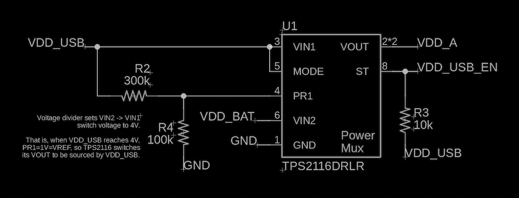
VDD_A is the "always on" power domain, which supplies power to the MSP430 and motion sensor. VDD_A is sourced by either the battery or USB, with USB taking preference. Switching between battery power and USB power is handled by a TPS2116 power mux:

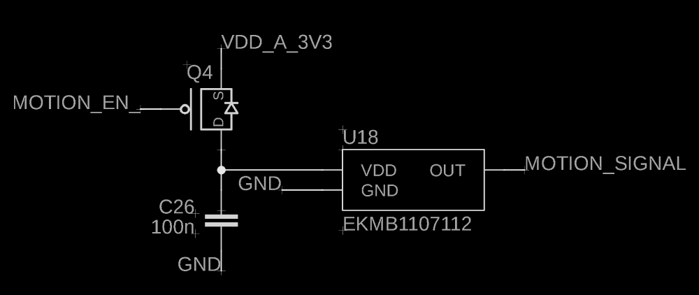
VDD_A, its power is gated by a PMOS transistor controlled by the MSP430, so that the motion sensor can be left unpowered if Photon isn't configured for motion detection: 
VDD_B
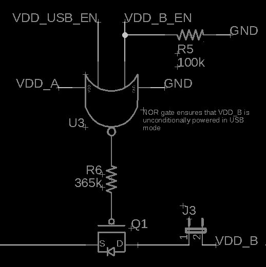
The VDD_B power domain provides power to everything else: ICE40 FPGA, image sensor, SDRAM, STM32, and SD card. VDD_B is gated by a single PMOS transistor, which is in turn controlled by a MSP430 GPIO. VDD_B is also unconditionally enabled when Photon is plugged into USB, since the STM32 handles USB comms and is powered by VDD_B.

VDD_B_1V8 / VDD_B_2V8
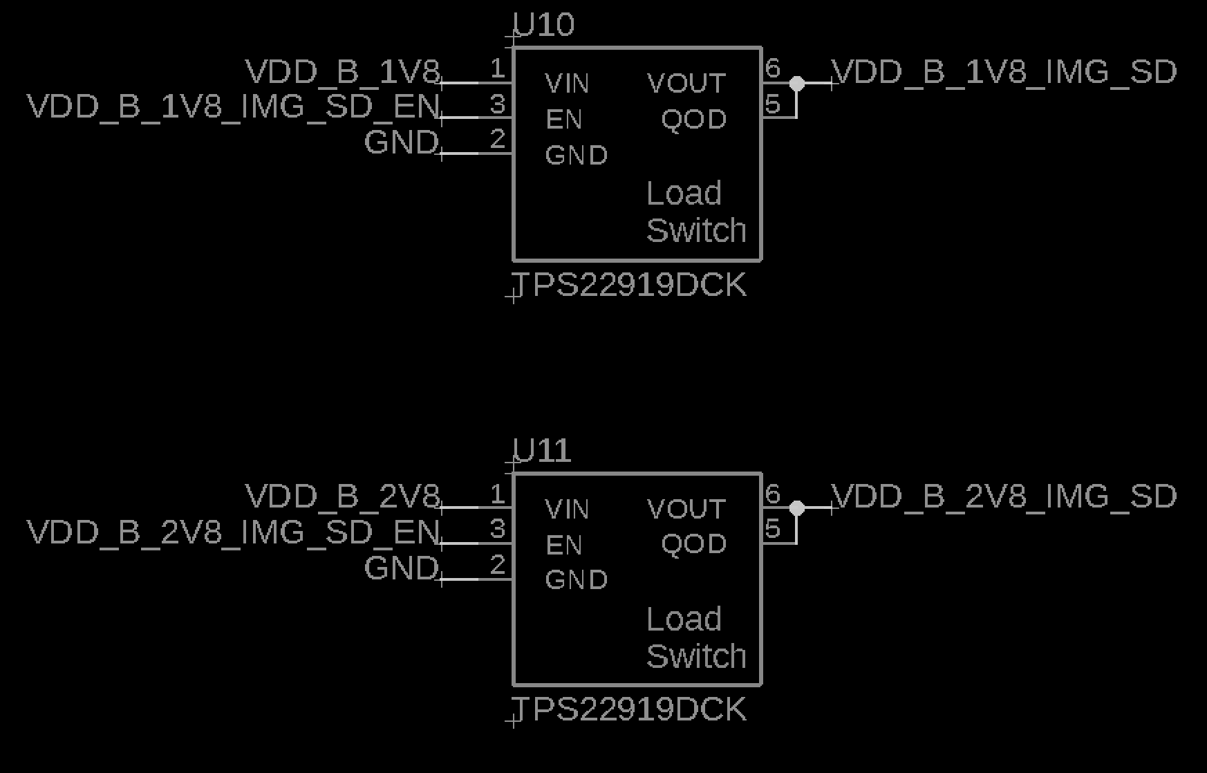
VDD_B is broken down further into the VDD_B_1V8 / VDD_B_2V8 subdomains, controlled by load switches, which are in turn controlled by MSP430 GPIOs: 